The spectroscopy laboratory provides the support for analysis of chemical, structural and physical properties of materials. Advanced instrumentation allows fundamental studies of condensed matter with high specificity to the surface processes. Such a specifity is a key in the study of novel systems synthesized by several growth means ( MBE, thermal evaporations, from solvents ...) on the surfaces like low dimensional adsorbates ( molecular and metallic chains , carbon nanotubes, nanoislands), novel materials ( diluted alloys, organic photovoltaic), and their behaviors under normal and extreme conditions ( surface melting).
Instrumentation includes:
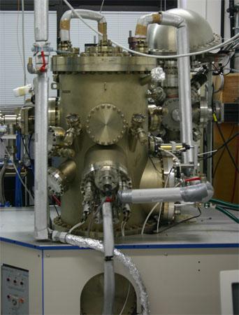
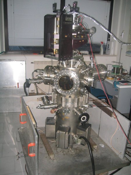
Ultra High vacuum apparatus with base pressure of 10-10 Torr.
UHV evaporators and molecular beams sources for thin films growth. The system is available for the growth of SiGe heterostructures possibly doped by Magnetic impurities (Mn).
|

|
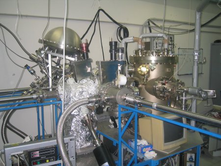
Electron analyser and radiation sources ( X-rays and UV) for core and valence levels photoemission spectroscopies.
High spatial and energy resolution allows determination of surface structures, semiconductor-metal electronic band offset, work function measurement. Chemical composition of the films can be also determined by sputtering by Ar ions.
|

|
|
UHV system for dedicated experiments in extreme conditions like in surface melting or carbonization of surfaces for C-based films, like diamond, carbon nanotubes, SiC films. Advanced control in gas inlet, temperature control. Electron spectroscopies are available for the analysis of the material properties.
|

|
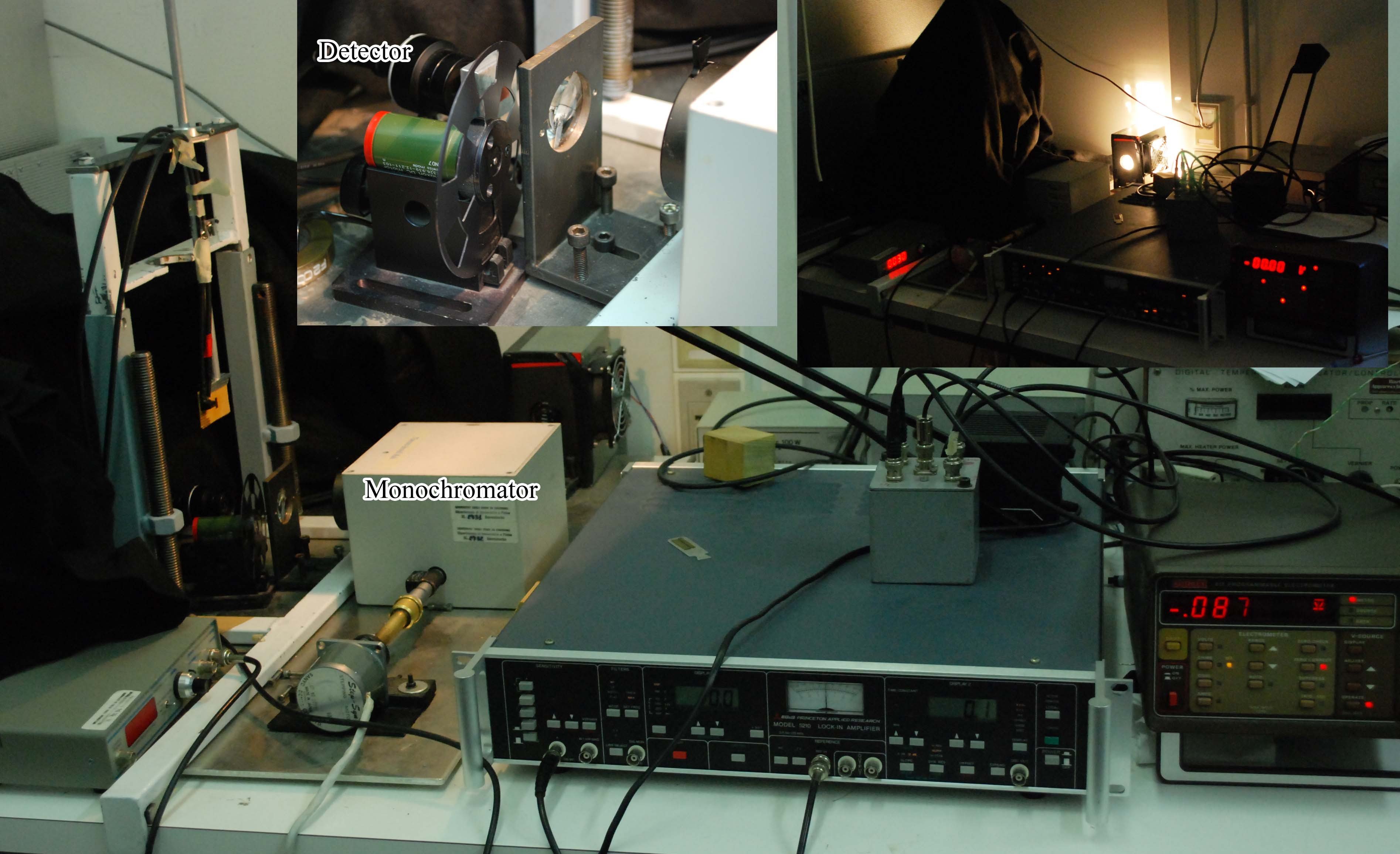
| Optical spectroscopies ( UV-VIS absorption and photoconductivity ) by means of lock-in technique for the determination of the absorption range and external quantum efficiency in photovoltaic devices. Electric characterization by means of an electrometer in a Lab-view computer controlled system.
|

|
|
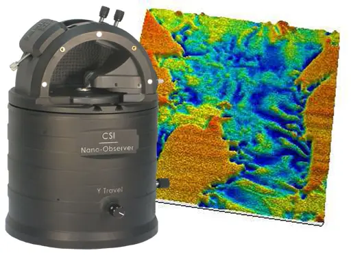
Apparatus for the determination of surface topography by atomic force probe in contact and non-contact mode.
|

|
|
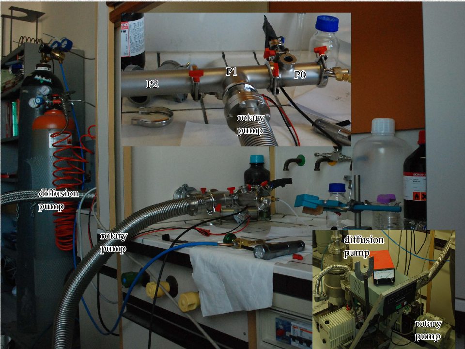
Apparatus for the growth of thin films from solutions for polymer and bio polymer based devices for optoelectronics by means of an electro-spray method making use of differential pumping system and high electric field assisted deposition.
|

|
